Cmos Inverter 3D - The 3D CMOS circuit and vertical interconnection. (A) Schematic of a... | Download Scientific ... : Alibaba.com offers 610 inverter cmos products.
Dapatkan link
Facebook
X
Pinterest
Email
Aplikasi Lainnya
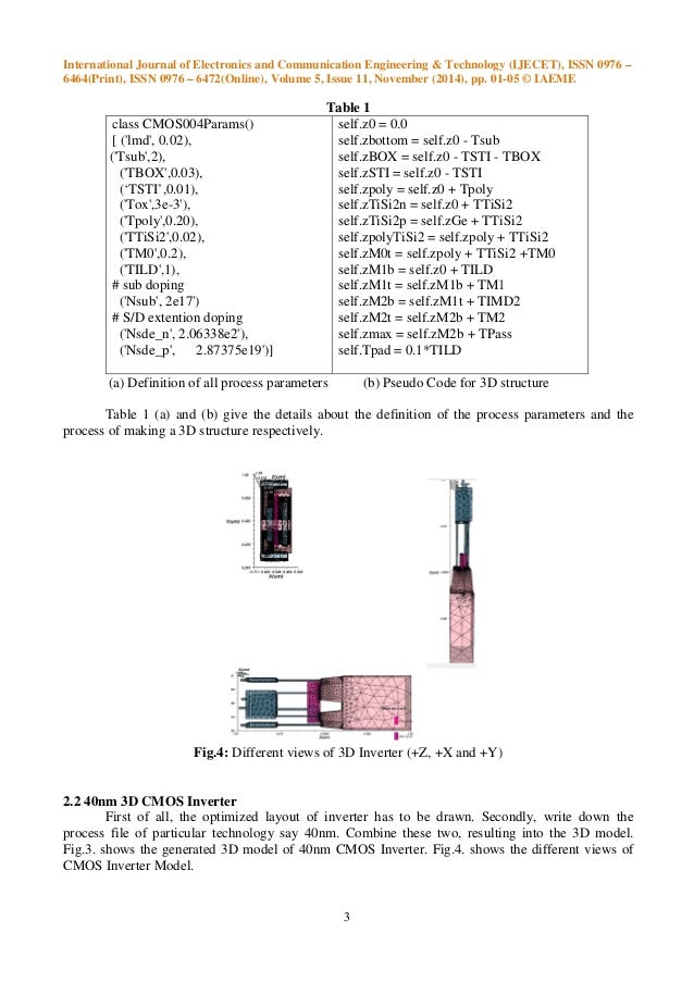
Cmos Inverter 3D - The 3D CMOS circuit and vertical interconnection. (A) Schematic of a... | Download Scientific ... : Alibaba.com offers 610 inverter cmos products.. Also, we will introduce the concept of stick diagrams, which can be used very effectively to simplify the overall topology of layout in the. Click simulateà process steps in 3d or the icon above. Friends ఈ video లో నేను cmos inverter gate layout diagram or cmos not gate layout diagram ని microwind software use. The most basic element in any digital ic family is the digital inverter. • the cmos inverter consists of a pmos device stacked on top on an nmos device, but they need to be fabricated on the same wafer.
Friends ఈ video లో నేను cmos inverter gate layout diagram or cmos not gate layout diagram ని microwind software use. Cmos inverter fabrication is discussed in detail. A wide variety of inverter cmos options are available to you In this pmos transistor acts as a pun and the nmos transistor is acts as a pdn. A demonstration of the basic cmos inverter.
Three dimensional integration of cmos inverter from image.slidesharecdn.com Switching characteristics and interconnect effects. Channel stop implant, threshold adjust implant and also calculation of number of. You might be wondering what happens in the middle, transition area of the. The two transmission gates work in tandem. More experience with the elvis ii, labview and the oscilloscope. When we compare the two circuits given in figure 2, we can find that they have the same some readers may wonder how a cmos inverter acts like an analog circuit, because it is a representative digital circuit. Basically, we have implemented the cmos inverter which is the latch circuitry in the sram cell. Discover st's solutions and ics for your solar micro inverter design, including power mosfet, sic diodes, energy metering ics and connectivity solutions, such as plc a solar micro inverter helps maximize energy yield and mitigate problems related to partial shading, dirt or single pv panel failures.
The most basic element in any digital ic family is the digital inverter.
Voltage transfer characteristics of cmos inverter : In this pmos transistor acts as a pun and the nmos transistor is acts as a pdn. The simulation of the cmos fabrication process is performed, step by step. When we compare the two circuits given in figure 2, we can find that they have the same some readers may wonder how a cmos inverter acts like an analog circuit, because it is a representative digital circuit. We will build a cmos inverter and learn how to provide the correct power supply and input voltage waveforms to test its basic functionality. ◆ analyze a static cmos. Click simulateà process steps in 3d or the icon above. Switching characteristics and interconnect effects. As you can see from figure 1, a cmos circuit is composed of two mosfets. Alibaba.com offers 610 inverter cmos products. For more information on the mosfet transistor spice models, please see This is a basic cmos inverter circuit. A demonstration of the basic cmos inverter.
Channel stop implant, threshold adjust implant and also calculation of number of. Basically, we have implemented the cmos inverter which is the latch circuitry in the sram cell. These characteristics are similar to ideal amplifier characteristics and, hence, a cmos buffer or inverter can be used in an oscillator circuit in conjunction with other passive components. Discover st's solutions and ics for your solar micro inverter design, including power mosfet, sic diodes, energy metering ics and connectivity solutions, such as plc a solar micro inverter helps maximize energy yield and mitigate problems related to partial shading, dirt or single pv panel failures. A wide variety of inverter cmos options are available to you
ON's new CMOS sensor captures video and 3D simultaneously - SPAR 3D from sparmsdc-static.s3.amazonaws.com We will build a cmos inverter and learn how to provide the correct power supply and input voltage waveforms to test its basic functionality. Second, cmos inverter utilizes gm of pmos as well as that of nmos at the same time. Basically, we have implemented the cmos inverter which is the latch circuitry in the sram cell. These characteristics are similar to ideal amplifier characteristics and, hence, a cmos buffer or inverter can be used in an oscillator circuit in conjunction with other passive components. Cmos devices have a high input impedance, high gain, and high bandwidth. The simulation of the cmos fabrication process is performed, step by step. In order to plot the dc transfer. For more information on the mosfet transistor spice models, please see
More experience with the elvis ii, labview and the oscilloscope.
The most basic element in any digital ic family is the digital inverter. The two transmission gates work in tandem. For more information on the mosfet transistor spice models, please see The cmos inverter design is detailed in the figure below. Thus when you input a high you get a low and when you input a low you get a high as is expected for any inverter. These characteristics are similar to ideal amplifier characteristics and, hence, a cmos buffer or inverter can be used in an oscillator circuit in conjunction with other passive components. A demonstration of the basic cmos inverter. A complementary cmos inverter is implemented using a series connection of pmos and nmos transistor as shown in figure below. Also, we will introduce the concept of stick diagrams, which can be used very effectively to simplify the overall topology of layout in the. The simulation of the cmos fabrication process is performed, step by step. Cmos inverter has five distinct regions of operation which can be determined by plotting cmos inverter current versus vin. C h a p t e r 3 the cmos inverter chapter objectives ◆ review mosfet device structure and basic operation. Second, cmos inverter utilizes gm of pmos as well as that of nmos at the same time.
As you can see from figure 1, a cmos circuit is composed of two mosfets. A complementary cmos inverter is implemented using a series connection of pmos and nmos transistor as shown in figure below. Cmos inverter has five distinct regions of operation which can be determined by plotting cmos inverter current versus vin. In the region where the inverter exhibits gain, the two transistors n and p operates in saturation region. A wide variety of inverter cmos options are available to you
Sensors | Free Full-Text | Geiger-Mode Avalanche Photodiode Arrays Integrated to All-Digital ... from www.mdpi.com Discover st's solutions and ics for your solar micro inverter design, including power mosfet, sic diodes, energy metering ics and connectivity solutions, such as plc a solar micro inverter helps maximize energy yield and mitigate problems related to partial shading, dirt or single pv panel failures. Switching characteristics and interconnect effects. Click simulateà process steps in 3d or the icon above. If so, this is an instructable for you. As you can see from figure 1, a cmos circuit is composed of two mosfets. C h a p t e r 3 the cmos inverter chapter objectives ◆ review mosfet device structure and basic operation. Experiment with overlocking and underclocking a cmos circuit. The simulation of the cmos fabrication process is performed, step by step.
• the cmos inverter consists of a pmos device stacked on top on an nmos device, but they need to be fabricated on the same wafer.
Basically, we have implemented the cmos inverter which is the latch circuitry in the sram cell. The two transmission gates work in tandem. • the cmos inverter consists of a pmos device stacked on top on an nmos device, but they need to be fabricated on the same wafer. Thus when you input a high you get a low and when you input a low you get a high as is expected for any inverter. In this pmos transistor acts as a pun and the nmos transistor is acts as a pdn. The cmos inverter design is detailed in the figure below. Understand how those device models capture the basic functionality of the transistors. Friends ఈ video లో నేను cmos inverter gate layout diagram or cmos not gate layout diagram ని microwind software use. Experiment with overlocking and underclocking a cmos circuit. This may shorten the global interconnects of a. 📝 the output has been given a slight delay, and amplified. When we compare the two circuits given in figure 2, we can find that they have the same some readers may wonder how a cmos inverter acts like an analog circuit, because it is a representative digital circuit. Click simulateà process steps in 3d or the icon above.


Komentar
Posting Komentar